Twin Creeks Tech turning silicon into thin-film PV
 The process of making most conventional photovoltaic (PV) cells requires a lot of energy and using a diamond saw to cut wafers out of larger pieces of silicon ingot, which results in dusty waste and results in wafers that are relatively thick at about 200 microns, thick enough that they’re not flexible.
But Twin Creeks Technologies has developed a means of peeling wafers 20 microns thick from larger slices of silicon in a process that produces almost no waste, a significantly thinner silicon wafer with all the benefits of a thicker wafer and the added benefit of flexibility, while reducing the amount of energy needed to produce such wafers.
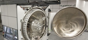
The company is now marketing its Hyperion proton knife system, which, when open, resembles a gigantic spoked wheel in a barrel. Basically, what it does is take thicker wafers, up to a few millimeters thick, and uses Proton Induced Exfoliation (PIE) to slice them into thinner wafers.
The process uses a 1.2-megavolt hydrogen energy beam, which penetrates the surface of the wafer with hydrogen ions, creating a uniform layer of hydrogen under the surface of the wafer at a set depth.
After wafers are saturated with hydrogen, they’re transferred to an oven where the heated hydrogen expands and peels off the 20-micron layer. The process is repeated until the donor wafer is itself the same thickness, said spokesperson Michael Kanellos.
“It takes about 18 minutes in total to embed the hydrogen,” Kanellos said.
Including the baking process, each donor wafer can produce 3 thinner wafers an hour, the Hyperion chamber holds 60 donor wafers in a giant rotational drum where the automated process occurs and produces 180 thinner wafers hourly.
The company experimented with the thickness of the wafers and found that 15- to 20- microns was the ideal thickness, because they retained all the attributes of thicker wafers.
Thinner wafers, however, can’t produce as much energy, Kanellos said.
Producing thinner layers of wafers means less silicon per completed cell, which reduces weight and helps manufacturers get more out of each ingot. Plus, even at 1.2 megavolts, the amount of power used to produce each wafer is much less, according to Kanellos.
“It takes about two years to work off the carbon for a normal solar cell, but it only takes 25 days to work it off here,” he said.
That’s because of the reduced energy use, but it also sheds some light on possible cost reductions of making such a cell.
The process is currently being used for monocrystalline silicon, but could also be used for Gallium Arsenide PV cells. The more expensive cells being used in spacecraft and high-concentrating PV devices. Kanellos explained that the technology also could be used for making wafers for LEDs and CMOS—camera—sensors.
Solar manufacturers are testing the process with their silicon wafers at Twin Creeks’ Mississippi facility. The company plans to sell six to 12 of the systems this year and hundreds after that, according to Kanellos.