Researchers develop super absorbent solar sponge
 Using nanoscale technologies, researchers at Caltech have developed a nano-structured material that can absorb light using optical resonance, which could drastically increase the amount of sun that thin-film-based photovoltaics can absorb. The devices can be tuned to absorb 70 percent of light across the visible spectrum.
With further research such a material could be added to existing forms of thin-film photovoltaics, increasing their conversion efficiency while retaining their thinness, which helps reduce cost. The research, led by Harry Atwater, a Caltech professor of applied physics and materials science, was recently published in Nature Communications.
“Being able to design optical properties at the nanoscale gives us the power to control how the sunlight interacts with the solar cell. High absorption using less and less material is the dream of every researcher in the photovoltaics field, as it will result in significant cost reductions and make solar cells competitive with carbon-based energy resources,” said Koray Aydin, a researcher on the project, who’s now an assistant professor of electrical engineering and computer science at Northwestern University.
Incorporating the technology into existing production lines is their ultimate goal with the research, Aydin said.
“Right now the absorption takes place in the metal, which is not useful for solar energy,” he said. “It is possible to design optical materials at the nanoscale yielding superior absorption and/or scattering properties that might yield broadband, polarization-independent, wide-angle light management characteristics which are essential for achieving the highest efficiency from a solar cell throughout the day.”
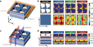
What’s unique about the material is that different parts of the structure absorb different spectrums of light, according to Aydin.
“We plotted the absorption as a function of position. The absorption takes place at different wavelengths within different locations inside the material,” he said. “Most of the absorption takes place in the top metal layer, sometimes at tips and bases, sometimes at the center. So we have control over where the light being absorbed and design all sorts of interesting optical materials.”
At this point, they’ve only worked with absorbing the spectrum of light between blue and red, according to Aydin.
“But it is possible to go beyond visible and extend the design to absorb at UV and infrared [wavelengths] depending on the type of the material and application,” he said.
The device can absorb light, but not convert it into electricity, Aydin said.
“However, using the design guidelines that we outlined in this study, we are now working on nano-structured silicon to achieve high absorption in ultra-thin silicon films,” he said. “We have promising results that we are not just ready to share with the public at this point.”
They have developed a 220-nanometer-thick silicon-film that can absorb as much sunlight as a film 25 times thicker, according to MIT’s Technology Review.
Image courtesy of Nature Communications.