Nano-designed structures create 18.2 percent efficient solar cell at NREL
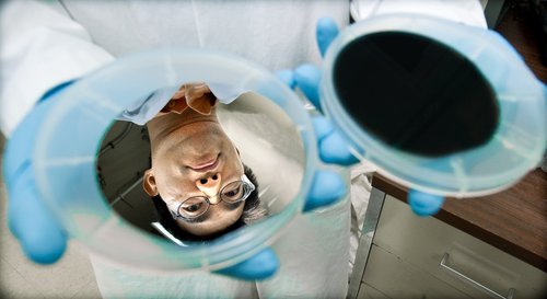
 Using a chemical nano-porous etching process, the National Renewable Energy Laboratory (NREL) was able to create an antireflective surface on silicon PV cells without using additional antireflection coating. The method could reduce the cost of adding anti-reflective layers to crystalline silicon-based photovoltaics.
Researchers at the laboratory, including Jihun Oh, Hao-Chih Yuan, and Howard Branz developed a nanostructured surface for black silicon photovoltaic cells, which are designed to absorb more light than conventional PV cells. “NREL’s nano-porous silicon suppresses the reflective loss and hence allows more sunlight into the solar cell to be converted into electricity,” Yuan said. “It performs better and has lower cost compared to conventional dielectric anti-reflection coatings. We envision the nano-porous silicon anti-reflection to be applicable to all type of crystalline silicon solar cells,” he said.
The nano-porous surface etched into the crystalline silicon eliminates abrupt interface and as a result eliminates reflection of the incident of light, according to Yuan. “While it is a fact that about half micrometer deep nano-porous surface is needed to suppress the reflection for wavelengths up to about one micrometer, this nano-porous structure does not alter the absorption property of crystalline silicon.” However, infrared light, won’t be absorbed because of silicon’s bandgap, regardless of the application of the nano-porous surface, he said.
To make the structures, the researchers made nano-islands of silver on a silicon wafer and immersed it briefly in liquids, according to NREL. The process made billions of nano-sized holes, smaller than the light wavelengths that hit them, keeping light from reflecting off the surface.
The etching is beyond small. “NREL’s chemical nano-porous etching consumes less than a micrometer of silicon at the surface in the case of 18.2% efficient silicon solar cell, Yuan said. “The etching depth can be tailored depending on the application. Nonetheless, this technology can be applied on thin silicon substrates couple of micrometer or above.”
Moving forward, the group will work to design the process to work with common industrial practices, according to Branz. After applying the technology in such a way, they will work towards getting the effiicency higher than 20 percent at which point he hoped the technology would be used by PV manufacturers.


