Plug-and-play solar? How about peel-and-stick solar?
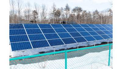
 The future of solar’s myriad of applications will be determined by a number of things, but all of them boil down to making solar easy to use and efficient enough to be practical. That’s why plug and play solar is important. But one of the other things that is becoming increasingly insight is the making sure the uses of solar are flexible. Researchers at Stanford University have just created peel-and-stick photovoltaics, using flexible PV, and in the process, perhaps creating one of the most flexible applications of solar, ever.
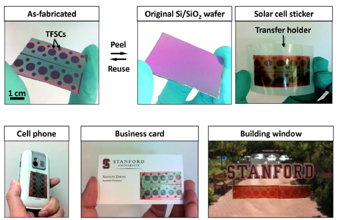
The research behind developing the peel-and-stick thin-film solar cells (TFSCs) was recently published in the December 20th issue of Scientific Reports. Chi Hwan Lee, a PhD candidate in mechanical engineering was lead author of the paper and Xiaolin Zheng, a Stanford assistant professor of mechanical engineering was its senior author. Their team developed what they called a first of its kind peel-and-stick application for thin-film PV cells. “We report a novel and versatile peel-and-stick process to directly build TFSCs on diverse previously inaccessible substrates, such as paper, plastic, cell phones, and buildings,” they said in the research.
The process results in a solar cell that can be applied to a surface in a tape-like fashion. With the final product the end-user or producer, simply peels the backing off and sticks it on like a bumper sticker. “It’s significant that we didn’t lose any of the original cell efficiency,” says Zheng.
“The peel-and-stick process, while preserving the TFSC performance, circumvents the fabrication challenges associated with the nonconventional substrates by separating the fabrication process with the final target substrate. These previously inaccessible substrates for TFSCs enable further reduction of the cost and weight, and endow TFSCs with flexibility and attachability to greatly broaden their application areas,” they explained.
In addition, the process they described allows the wafer the PV cell is developed on to be reused. In the process a 300-nanometer nickel film is deposited on a silicon/silicon dioxide wafer. “The thin-film solar cells are then deposited on a nickel layer utilizing standard fabrication techniques, and covered with a layer of protective polymer. A thermal release tape is then attached to the top of the thin-film solar cells to augment their transfer off of the production wafer and onto a new substrate,” according to Stanford.
After that process, the assembly is submerged in water at room temperature and the edge of the thermal release tape is peeled back slightly. The process allows water to penetrate between the nickel and silicon dioxide layers, splitting them and freeing the PV device from the silicon, but leaving it attached to thermal tape. The thermal tape is heated to 90°C for several seconds, attached to an adhesive substance and then the thermal tape can be removed, leaving an intact PV device that can be applied almost anything from paper to windows to the back of a cell phone.
Thus far they have only applied the process to this specific type of PV, but they believe the process has further application. “We believe that the peel-and-stick process can be applied to other kinds of TFSCs and thin film electronics as well,” they wrote in the research paper. The process could also yield flexible circuits, for instance.